electric field energy band diagram
Energy band diagrams for isolated ZnO and Cu2O electrodeposited at. 9 Images about Energy band diagrams for isolated ZnO and Cu2O electrodeposited at : Conduction In Conductors And Semiconductors | Electrical engineering, Crystals and Band Theory | Boundless Chemistry and also (a) Structure of the perovskite LED device. (b) Energy band alignment.
Energy Band Diagrams For Isolated ZnO And Cu2O Electrodeposited At
 www.researchgate.net
cu2o zno nrs pec heterostructures electrodeposited gsh biosensing
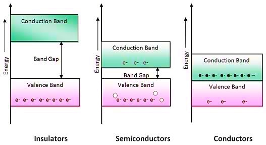
Crystals And Band Theory | Boundless Chemistry
 courses.lumenlearning.com
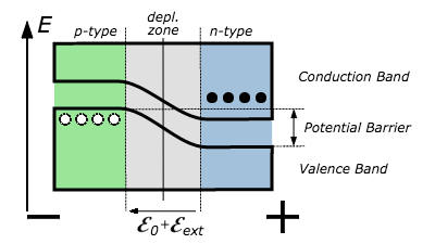
junction chemistry reverse band diagram biased theory drift electric detectors space current across field boundless potential bands doping pn bias
2: Schematic Showing Magnetic Hysteresis Loop Of A Ferromagnetic
 www.researchgate.net
hysteresis ferromagnetic
Energy Band Structure Of GaAs, Electrons In Γ Valley Have Light
 www.researchgate.net
NIST Finds That Two Graphene Layers May Be Better Than One
 www.nextbigfuture.com
graphene bilayer diagram layers energy band measurements nist finds quantum hall bernal stacked better than schematics
KIT - CFN
 www.cfn.kit.edu
diagram hall spin quantum effect phase cfn kit b2 interferometer edu
(a) Structure Of The Perovskite LED Device. (b) Energy Band Alignment
 www.researchgate.net
perovskite
Gate-induced Drain Leakage In The MOSFETs. (a) A Schematic View Of The
 www.researchgate.net
leakage induced mosfets schematic overlapped
Conduction In Conductors And Semiconductors | Electrical Engineering
 electricallive.com
conductors semiconductors band conduction classification energy diagram based material insulators gap theory insulator physics questions differ stack following
Crystals and band theory. Cu2o zno nrs pec heterostructures electrodeposited gsh biosensing. Conductors semiconductors band conduction classification energy diagram based material insulators gap theory insulator physics questions differ stack following